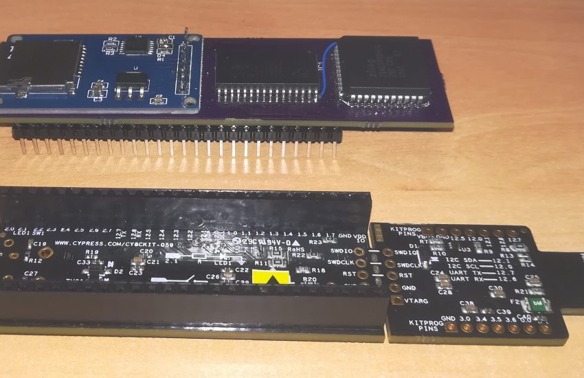
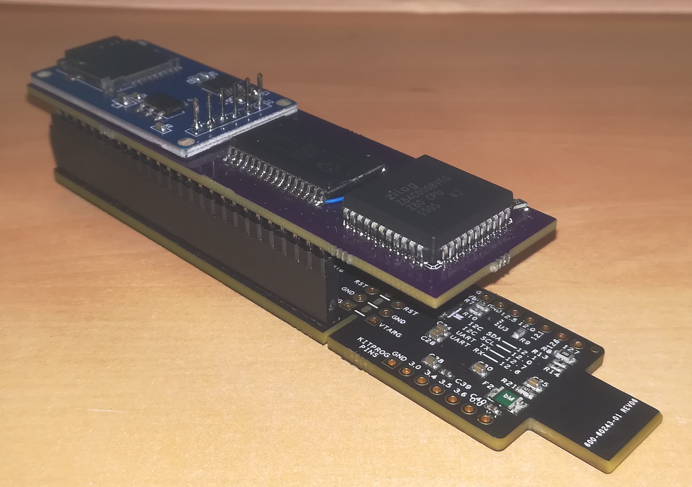
A new iteration of the concept : Romless z80sbc with a PSoC5 module that is doing bootloader/glue logic/serial output & sd-card interface.
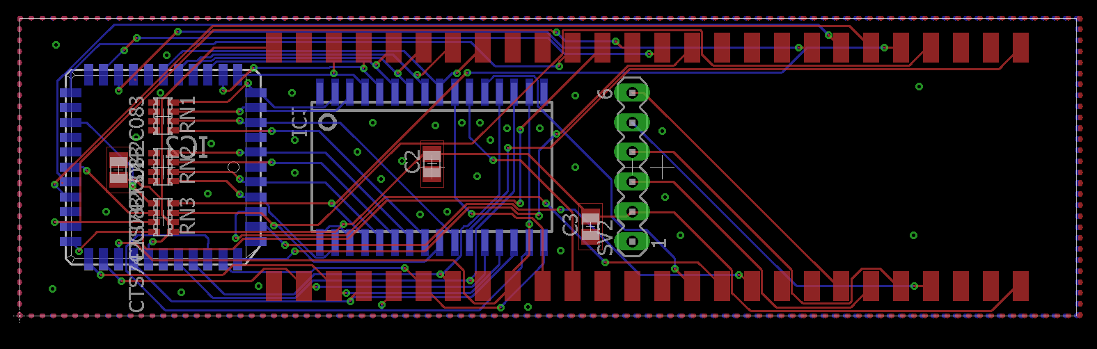
This time I designed a PBC for the project (OSH Park)
The BOM is :
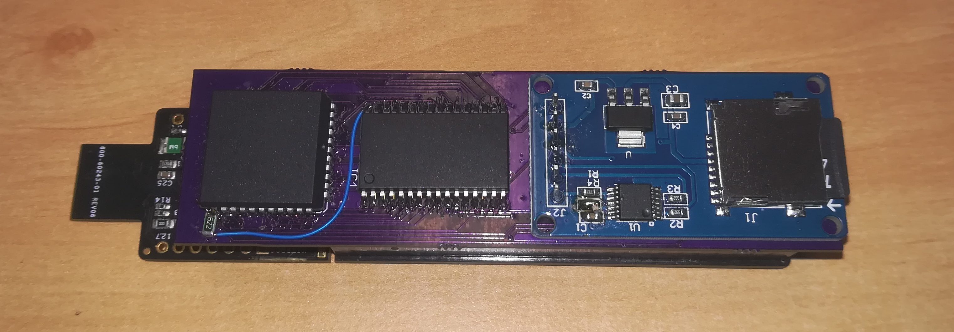
- Z80 CPU (plcc)
- 128k Sram
- some resistors (resistor arrays)
- some capacitors (decoupling)
- a microSD card breakout board (SV2 on schematic)
- a PSoC5 module (cy8ckit-059, around 10 euros)

Some explanations :
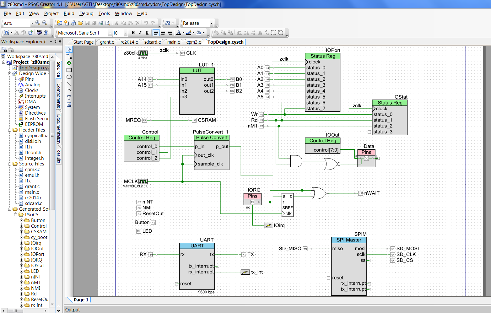
- Almost all signals are interconnected between Z80 and PSoC5+SRAM
- but since I/Os are limited on PSoC5 module, only A0-A5 and A14-15 are in fact connected.
- It limits IO port decoding since A7 & A6 are not present, thus OUT to port 0xA8 would be seen as OUT to 0x28… not a big problem with the Roms I wanted to test.
- A6-A13 are pull-down, this is important for Bootloader (see just after)
- When a Z80 access is done on an IO port, WAIT signal is used to give time to the PSoC to handle the request (Bootloader byte / Serial In/Out / SDcard access / Interrupt ?)
- Memory accesses are done directly to the SRAM, without PSoC intervention – only a LUT table is used for the memory bank switching (normal mode is 0x0000-0xFFFF mapped to RAM, bank 1 maps RAM 0x10000 to 0x4000-0xBFFF, bank 2 maps 0x18000 to 0x4000-0xBFFF)
- The design is ROMless, so a specific bootloader process is used to fill the RAM at boot :
- The Z80 is put in RESET mode – during RESET, Address bus and Data bus is in high impedance mode
- RD and WR are still driven, so a resistor is needed between the Z80 and Ram/PSoC to allow the PSoC to drive those signals during the RESET/Bootloader phase.
- PSoC inputs (A0-A5, Data, RD/WR) are dynamically changed to Outputs – A6-A13 will be pulled low – B0-B2 will be forced low too (bypassing the LUT output), so A14-A16 on the SRAM will be low. Read/Write to SRAM will be limited to 0x0000-0x003F (64 bytes).
- A small Z80 program is directly written to RAM
- There is a verification phase (Data are switched back to inputs on PSoC5) to check the bootloader.
- The Z80 is put out of RESET, and starts running from 0x0000…
- The bootloader program relocates itself from 0x0000-0x00xx (xx=~24) to 0x4000, and gets additional bytes from port 0xFF (it writes them from 0x0000 to 0x3FFF – if less than 16K, then ‘xx’ is output).
- At the end, bootloader jumps back to 0x00
- the Z80 now executes the code it received on port 0xFF…
- IO access to serial chips (SIO/ACIA) is translated by the PSoC to UART commands
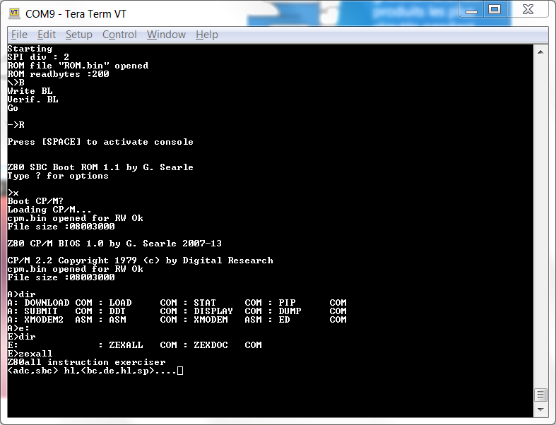
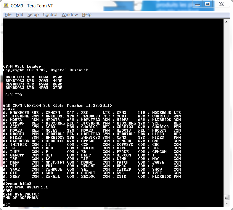
- IO access to storage (for CPM 2.2/3.x) is translated by PSOC to FatFS access on cpm.bin or cpm3.bin read/writes – thus is is quite easy to change/create disks as it is only a file on the uSD on a regular FAT filesystem.
- Interrupt using IM2 and SIO is supported (needed for Grant Searle mode)
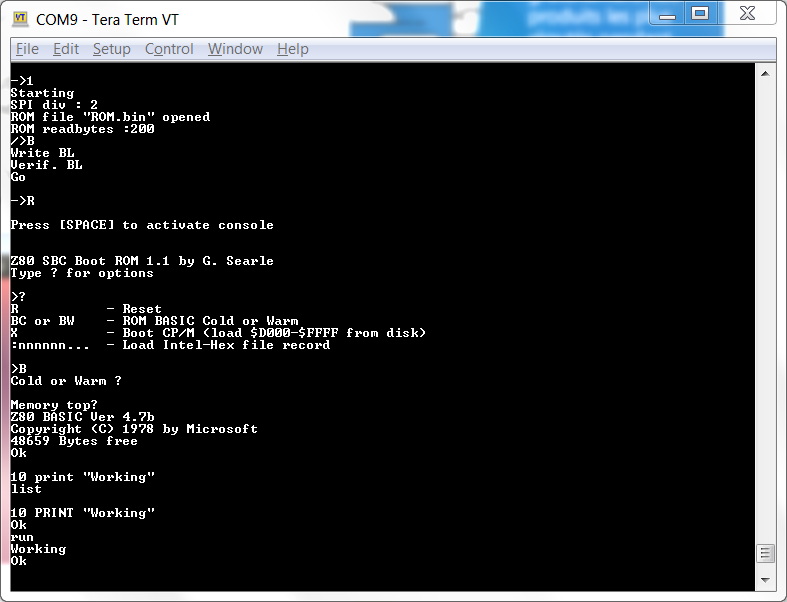
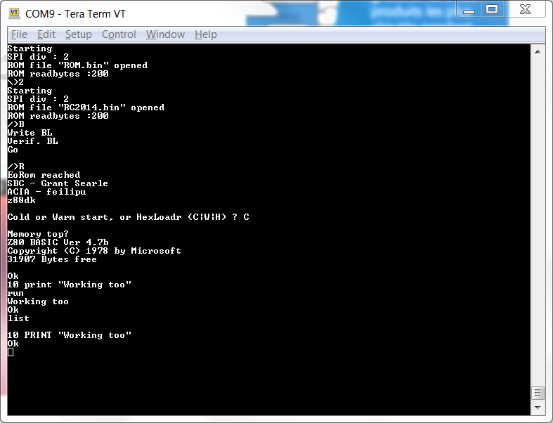
- At boot, the PSoC program waits for some basic commands on the console: at the moment, ‘1’ , ‘2’ , ‘3’ are selecting Grant Searle Rom, RC2014 Rom or CPM3 test ‘cpmldr.com’ respectively (each one with its specific code for IO handling/main loop), ‘B’ installs the small bootloader code on the SRAM and ‘R’ starts the Z80 by releasing RESET.
On this platform I was able to run, without re-programming to PSoC and using the same sdcard :
- Grant Searle’s ROM with Basic & CPM2.2 (without modifications)
- RC2014 Basic Rom
- A preliminary test CPM3 based on sources from S100computers.com
I was able to have a stable system @ 16Mhz, with a regular Z84C0008VEG (8Mhz) and all ZEXALL tests passed in ~49 minutes.


Cypress PSoC Creator project file :
Eagle Schematic and Board :
Notes on HW/PCB :
- BUG : a pull-up resistor is missing on Z80 BUSREQ signal.
- C7 on the PSoC module needs to be removed (that capacitor was put for analog
- On uSD breakout board, I had to change R4 to make it a pull-up on MISO line (found a schematic on http://file.vishnumaiea.in/hard/micro-sd/Catalex-mSD-Card-Module_SCH.png)
Misc. Data to put on uSD :
Not yet released… need to check if redistribution is allowed
Hello, what resistor value did you use between RD/WR on the Z80 and the SRAM/PSOC? How did you choose this?
I guess I took 1k as resistor, it has the same functionality as resistors on the data bus of a ZX81 (see Grant Searle’s pages), i.e. being able to force the level from the PSOC, to drive the SRAM, without hurting the Z80 outputs.
In this version of my experiments with Z80/PSoC, the problem was that during a Reset, address/data buses are high impedance, but Rd/Wr are not…
Nice to have some feedback/questions – good luck.